Legal Representation
Attorney
Tomoko Nakajima
USPTO Deadlines
Next Deadline
32 days remaining
NOA E-Mailed - SOU Required
Due Date
January 22, 2026
Extension Available
Until July 22, 2026
Application History
22 events| Date | Code | Type | Description | Documents |
|---|---|---|---|---|
| Nov 21, 2025 | EISU | I | TEAS STATEMENT OF USE RECEIVED | Loading... |
| Jul 22, 2025 | NOAM | E | NOA E-MAILED - SOU REQUIRED FROM APPLICANT | Loading... |
| May 27, 2025 | NPUB | E | OFFICIAL GAZETTE PUBLICATION CONFIRMATION E-MAILED | Loading... |
| May 27, 2025 | PUBO | A | PUBLISHED FOR OPPOSITION | Loading... |
| May 21, 2025 | NONP | E | NOTIFICATION OF NOTICE OF PUBLICATION E-MAILED | Loading... |
| Apr 26, 2025 | CNSA | P | APPROVED FOR PUB - PRINCIPAL REGISTER | Loading... |
| Apr 26, 2025 | XAEC | I | EXAMINER'S AMENDMENT ENTERED | Loading... |
| Apr 26, 2025 | GNEN | O | NOTIFICATION OF EXAMINERS AMENDMENT E-MAILED | Loading... |
| Apr 26, 2025 | GNEA | F | EXAMINERS AMENDMENT E-MAILED | Loading... |
| Apr 26, 2025 | CNEA | R | EXAMINERS AMENDMENT -WRITTEN | Loading... |
| Apr 24, 2025 | TEME | I | TEAS/EMAIL CORRESPONDENCE ENTERED | Loading... |
| Apr 23, 2025 | CRFA | I | CORRESPONDENCE RECEIVED IN LAW OFFICE | Loading... |
| Apr 23, 2025 | TROA | I | TEAS RESPONSE TO OFFICE ACTION RECEIVED | Loading... |
| Feb 26, 2025 | XELG | O | APPLICATION EXTENSION GRANTED/RECEIPT PROVIDED | Loading... |
| Feb 26, 2025 | XELR | I | APPLICATION EXTENSION TO RESPONSE PERIOD - RECEIVED | Loading... |
| Nov 29, 2024 | GNRN | O | NOTIFICATION OF NON-FINAL ACTION E-MAILED | Loading... |
| Nov 29, 2024 | GNRT | F | NON-FINAL ACTION E-MAILED | Loading... |
| Nov 29, 2024 | CNRT | R | NON-FINAL ACTION WRITTEN | Loading... |
| Nov 29, 2024 | DOCK | D | ASSIGNED TO EXAMINER | Loading... |
| Nov 17, 2024 | MDSC | E | NOTICE OF DESIGN SEARCH CODE E-MAILED | Loading... |
| Nov 17, 2024 | NWOS | I | NEW APPLICATION OFFICE SUPPLIED DATA ENTERED | Loading... |
| May 15, 2024 | NWAP | I | NEW APPLICATION ENTERED | Loading... |
Detailed Classifications
Class 001
Unprocessed ultraviolet-curable polymer resins for use in the manufacture of semiconductors; unprocessed synthetic resins for use in the manufacture of semiconductors; unprocessed synthetic resins for use in forming bumps on a surface of semiconductor wafers before applying a protective tape to the surface
Class 017
Semi-processed synthetic resins for use in semiconductor manufacturing processes; semi-processed synthetic resins for use in forming bumps on a surface of semiconductor wafers before applying a protective tape to the surface; semi-processed ultraviolet-curable polymer resins for use in semiconductor manufacturing processes; semi-processed ultraviolet-curable polymer resins for use in the manufacture of semiconductors; synthetic resins in liquid state as semi-processed form for use in the manufacture of semiconductors products, with polymerization initiators added thereto.
Additional Information
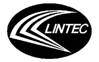
Design Mark
The mark consists of the stylized wording "LINTEC" located at the right side in an oval and triple depicted letters "L" in the form of a chevron located at the left side in the oval.
Color Claim
Color is not claimed as a feature of the mark.
Classification
International Classes
001
017