Legal Representation
Attorney
Shintaro Yamada
USPTO Deadlines
Next Deadline
1746 days remaining
Section 71 Declaration Due (Principal Register 66a) (Based on registration date 20241008)
Due Date
October 08, 2030
Grace Period Ends
April 08, 2031
Additional deadlines exist. Contact your attorney for complete deadline information.
Application History
38 events| Date | Code | Type | Description | Documents |
|---|---|---|---|---|
| Dec 18, 2025 | TCCA | I | TEAS CHANGE OF CORRESPONDENCE RECEIVED | Loading... |
| Dec 18, 2025 | ECDR | I | TEAS CHANGE OF DOMESTIC REPRESENTATIVES ADDRESS | Loading... |
| Dec 18, 2025 | ARAA | I | ATTORNEY/DOM.REP.REVOKED AND/OR APPOINTED | Loading... |
| Dec 18, 2025 | REAP | I | TEAS REVOKE/APP/CHANGE ADDR OF ATTY/DOM REP RECEIVED | Loading... |
| Apr 4, 2025 | FINO | P | FINAL DECISION TRANSACTION PROCESSED BY IB | Loading... |
| Mar 14, 2025 | FICS | P | FINAL DISPOSITION NOTICE SENT TO IB | Loading... |
| Mar 14, 2025 | FIMP | P | FINAL DISPOSITION PROCESSED | Loading... |
| Jan 8, 2025 | FICR | P | FINAL DISPOSITION NOTICE CREATED, TO BE SENT TO IB | Loading... |
| Oct 8, 2024 | NRCC | E | NOTICE OF REGISTRATION CONFIRMATION EMAILED | Loading... |
| Oct 8, 2024 | R.PR | A | REGISTERED-PRINCIPAL REGISTER | Loading... |
| Aug 17, 2024 | OPNX | P | NOTIFICATION OF POSSIBLE OPPOSITION - PROCESSED BY IB | Loading... |
| Jul 31, 2024 | OPNS | P | NOTIFICATION OF POSSIBLE OPPOSITION SENT TO IB | Loading... |
| Jul 31, 2024 | OPNR | P | NOTIFICATION OF POSSIBLE OPPOSITION CREATED, TO BE SENT TO IB | Loading... |
| Jul 23, 2024 | NPUB | E | OFFICIAL GAZETTE PUBLICATION CONFIRMATION E-MAILED | Loading... |
| Jul 23, 2024 | PUBO | A | PUBLISHED FOR OPPOSITION | Loading... |
| Jul 3, 2024 | NONP | E | NOTIFICATION OF NOTICE OF PUBLICATION E-MAILED | Loading... |
| Jun 20, 2024 | CNSA | O | APPROVED FOR PUB - PRINCIPAL REGISTER | Loading... |
| Jun 17, 2024 | TEME | I | TEAS/EMAIL CORRESPONDENCE ENTERED | Loading... |
| Jun 17, 2024 | CRFA | I | CORRESPONDENCE RECEIVED IN LAW OFFICE | Loading... |
| Jun 17, 2024 | TROA | I | TEAS RESPONSE TO OFFICE ACTION RECEIVED | Loading... |
| Jan 9, 2024 | GNRN | O | NOTIFICATION OF NON-FINAL ACTION E-MAILED | Loading... |
| Jan 9, 2024 | GNRT | O | NON-FINAL ACTION E-MAILED | Loading... |
| Jan 9, 2024 | CNRT | R | NON-FINAL ACTION WRITTEN | Loading... |
| Dec 22, 2023 | TEME | I | TEAS/EMAIL CORRESPONDENCE ENTERED | Loading... |
| Dec 21, 2023 | CRFA | I | CORRESPONDENCE RECEIVED IN LAW OFFICE | Loading... |
| Dec 21, 2023 | TROA | I | TEAS RESPONSE TO OFFICE ACTION RECEIVED | Loading... |
| Oct 25, 2023 | ATRV | O | ATTORNEY REVIEW COMPLETED | Loading... |
| Oct 25, 2023 | LIME | X | LIMITATION FROM THE IB - REQUEST EXAM REVIEW | Loading... |
| Jul 30, 2023 | LIMG | M | LIMITATION OF GOODS RECEIVED FROM IB | Loading... |
| Jul 26, 2023 | RFNT | P | REFUSAL PROCESSED BY IB | Loading... |
| Jul 5, 2023 | RFCS | P | NON-FINAL ACTION MAILED - REFUSAL SENT TO IB | Loading... |
| Jul 5, 2023 | RFRR | P | REFUSAL PROCESSED BY MPU | Loading... |
| May 23, 2023 | RFCR | E | NON-FINAL ACTION (IB REFUSAL) PREPARED FOR REVIEW | Loading... |
| May 22, 2023 | CNRT | R | NON-FINAL ACTION WRITTEN | Loading... |
| May 15, 2023 | DOCK | D | ASSIGNED TO EXAMINER | Loading... |
| Mar 7, 2023 | MAFR | O | APPLICATION FILING RECEIPT MAILED | Loading... |
| Mar 3, 2023 | NWOS | I | NEW APPLICATION OFFICE SUPPLIED DATA ENTERED | Loading... |
| Mar 2, 2023 | REPR | M | SN ASSIGNED FOR SECT 66A APPL FROM IB | Loading... |
Detailed Classifications
Class 007
Semiconductor manufacturing equipment, namely, semiconductor manufacturing machines, and semiconductor wafer processing equipment; machine couplings and transmission components and machine elements in the nature of shock prevention devices for semiconductor manufacturing equipment; semiconductor manufacturing machines and components thereof; semiconductor manufacturing machines and semiconductor exposure apparatuses for use in manufacture, and structural components thereof; positioning devices for semiconductor manufacturing equipment, namely, ball transfer units, and components thereof, namely, bearings, as parts of machines; hydraulic and pneumatic controls for semiconductor manufacturing equipment, and components thereof, namely, hydraulic valves being parts of machines, and oil-water separators for pneumatic controls being parts of machines; machines for manufacturing semiconductor equipment, semiconductor manufacturing machine components and appendages being parts of semiconductor manufacturing machines; semiconductor wafer processing machines and equipment, and structural components thereof; robots for manufacturing semiconductors, and structural components and appendages in the nature of structural parts thereof; semiconductor wafer processing equipment and structural components thereof; wafer manufacturing equipment for semiconductor manufacturing; semiconductor element manufacturing machines and exposure apparatuses for use in manufacture; semiconductor element manufacturing equipment, namely, machines therefor; integrated circuit manufacturing equipment, namely, machines therefor, and components thereof; stacked semiconductor chips manufacturing equipment, namely, machines for manufacturing stacked semiconductor chips; machines for nanoimprint lithography (NIL) for semiconductor manufacturing; equipment for manufacturing and processing microelectromechanical systems (MEMS), namely, electromechanical manufacturing and marking machines and components and appendages in the nature of parts thereof; equipment for cleaning microelectromechanical systems (MEMS), namely, dust removing installations for cleaning purposes, and components and appendages in the nature of parts thereof; cleaning devices for semiconductor manufacturing, namely, cleaning machines for semiconductor manufacturing machines; devices in the nature of machines for mounting IC chips on circuit boards; plasma etching machines; semiconductor exposure devices, namely, apparatus for use in manufacture; semiconductor cutting devices being parts of machines; semiconductor polishing devices being parts of machines; semiconductor plating devices being parts of machines; semiconductor etching devices being parts of machines; semiconductor thin-film formation devices being parts of machines; none of the aforementioned goods being 3D printers or machines for moulding plastics, or parts or fittings thereof
Class 037
Repair and maintenance of semiconductor manufacturing equipment, and providing information related thereto; repair and maintenance of semiconductor manufacturing machines, and providing information related thereto; repair and maintenance of semiconductor manufacturing machines and apparatuses, and providing information related thereto; repair and maintenance of positioning devices for semiconductor manufacturing equipment, and providing information related thereto; repair and maintenance of control devices for semiconductor manufacturing equipment, and providing information related thereto; repair and maintenance of semiconductor product manufacturing equipment, and providing information related thereto; repair and maintenance of semiconductor processing machines and apparatuses, and providing information related thereto; repair and maintenance of robots for manufacturing semiconductors, and providing information related thereto; repair and maintenance of semiconductor wafer processing equipment, and providing information related thereto; repair and maintenance of wafer manufacturing equipment for semiconductor manufacturing, and providing information related thereto; repair and maintenance of semiconductor element manufacturing machines and apparatuses, and providing information related thereto; repair and maintenance of semiconductor element manufacturing equipment, and providing information related thereto; repair and maintenance of integrated circuit manufacturing equipment, and providing information related thereto; repair and maintenance of stacked semiconductor chips manufacturing equipment, and providing information related thereto; repair and maintenance of machines for nanoimprint lithography (NIL) for semiconductor manufacturing, and providing information related thereto; repair and maintenance of equipment for manufacturing and processing microelectromechanical systems (MEMS), and providing information related thereto; repair and maintenance of equipment for cleaning microelectromechanical systems (MEMS), and providing information related thereto; repair and maintenance of cleaning devices for semiconductor manufacturing, and providing information related thereto; repair and maintenance of devices for mounting IC chips on circuit boards, and providing information related thereto; repair and maintenance of wafer foreign matter inspection devices for semiconductor manufacturing, and providing information related thereto; repair and maintenance of plasma etching machines, and providing information related thereto; repair and maintenance of semiconductor exposure devices, and providing information related thereto; repair and maintenance of semiconductor cutoff devices, and providing information related thereto; repair and maintenance of semiconductor polishing devices, and providing information related thereto; repair and maintenance of semiconductor plating devices, and providing information related thereto; repair and maintenance of semiconductor etching devices, and providing information related thereto; repair and maintenance of semiconductor thin-film formation devices, and providing information related thereto; repair and maintenance of semiconductor drying devices, and providing information related thereto; cleaning of machines and apparatuses for semiconductor manufacturing; cleaning of semiconductor manufacturing equipment; installation work of semiconductor testing equipment, and providing information related thereto; installation work of semiconductor manufacturing equipment, and providing information related thereto; repair and maintenance of electronic machines and apparatuses, and providing information related thereto; installation work, repair, and maintenance of computer hardware, and providing information related thereto; none of the aforementioned services being intended for 3D printers or for machines for moulding plastics, or parts thereof
Additional Information
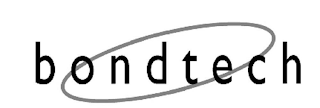
Design Mark
The mark consists of the stylized wording "BONDTECH" combined with an oval outline.
Classification
International Classes
007
037
Disclaimers
The following terms have been disclaimed and are not claimed as part of the trademark:
Specific Disclaimer
"BOND TECH" for Semiconductor manufacturing equipment, namely, semiconductor manufacturing machines, and semiconductor wafer processing equipment; semiconductor manufacturing machines and components thereof; semiconductor manufacturing machines and structural components thereof; machines for manufacturing semiconductor equipment, semiconductor manufacturing machine components and appendages being parts of semiconductor manufacturing machines; semiconductor wafer processing machines and equipment, and structural components thereof; robots for manufacturing semiconductors, and structural components and appendages in the nature of structural parts thereof; semiconductor wafer processing equipment and structural components thereof; wafer manufacturing equipment for semiconductor manufacturing; semiconductor element manufacturing machines; semiconductor element manufacturing equipment, namely, machines therefor; integrated circuit manufacturing equipment, namely, machines therefor, and components thereof; stacked semiconductor chips manufacturing equipment, namely, machines for manufacturing stacked semiconductor chips; equipment for manufacturing and processing microelectromechanical systems (MEMS), namely, electromechanical manufacturing machines and components and appendages in the nature of parts thereof; semiconductor plating devices being parts of machines; semiconductor thin-film formation devices being parts of machines, in International Class 7, and Repair and maintenance of semiconductor manufacturing equipment, and providing information related thereto; repair and maintenance of semiconductor manufacturing machines, and providing information related thereto; repair and maintenance of semiconductor manufacturing machines and apparatuses, and providing information related thereto; repair and maintenance of semiconductor product manufacturing equipment, and providing information related thereto; repair and maintenance of semiconductor processing machines and apparatuses, and providing information related thereto; repair and maintenance of robots for manufacturing semiconductors, and providing information related thereto; repair and maintenance of semiconductor wafer processing equipment, and providing information related thereto; repair and maintenance of wafer manufacturing equipment for semiconductor manufacturing, and providing information related thereto; repair and maintenance of semiconductor element manufacturing machines and apparatuses, and providing information related thereto; repair and maintenance of semiconductor element manufacturing equipment, and providing information related thereto; repair and maintenance of integrated circuit manufacturing equipment, and providing information related thereto; repair and maintenance of stacked semiconductor chips manufacturing equipment, and providing information related thereto; repair and maintenance of equipment for manufacturing and processing microelectromechanical systems (MEMS), and providing information related thereto; repair and maintenance of devices for mounting IC chips on circuit boards, and providing information related thereto; repair and maintenance of semiconductor plating devices, and providing information related thereto; repair and maintenance of semiconductor thin-film formation devices, and providing information related thereto; repair and maintenance of electronic machines and apparatuses, and providing information related thereto in International Class 37